The complete guide to PCB pad :types, size, spacing, repair and
$ 7.99
4.9(733)In stock
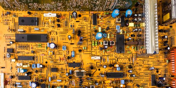
Soldering is one of the most important processes in PCBA processing. On printed circuit boards, electrical connections to all components are made via PCB pads. The PCB pads are a very critical part of the PCB that determines where components are soldered on the PCB.The size, shape, and position of pads in a PCB directly depend on the manufacturing quality of the board. Today we will take a look at the PCB pad in SMT soldering. Soldering is one of the most important processes in PCBA processing. On printed circuit boards, electrical connections to all components are made via PCB pad.
Getting to know PCB terminal blocks : function, material and sizes - IBE Electronics
An ultimate guide to PCB gold fingers - IBE Electronics
How to maintain and clean PCB stencils for consistent performance? - IBE Electronics
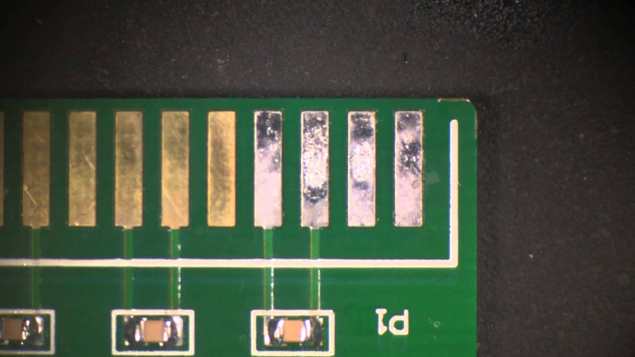
How To Repair Damaged /Missing PCB Pads INVISIBLE Fix, 45% OFF
The complete guide to PCB pad :types, size, spacing, repair and comparison - IBE Electronics
How To Repair Damaged /Missing PCB Pads ? - RAYPCB
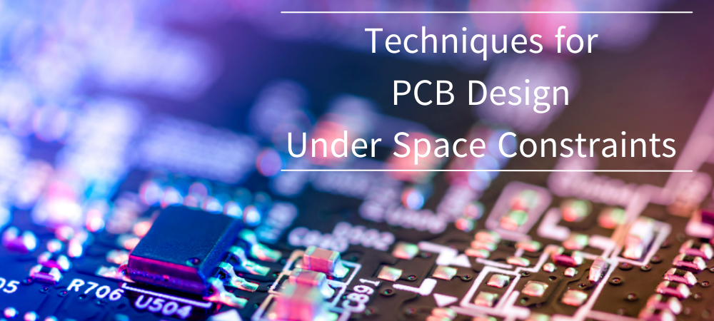
Techniques for PCB Design Under Space Constraints
How Do Circuit Boards Work: A Comprehensive Guide to the Heart of Electronics
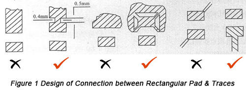
Design Requirement of SMT PCBs Part Two: Settings of Pad-Trace Connection, Thru-Holes, Test Point, Solder Mask and Silkscreen
An ultimate guide to PCB gold fingers - IBE Electronics


:max_bytes(150000):strip_icc()/exfoliating-pads-primary-8fcf5f84adea4dd3a5c6cfb3b80dbde3.jpg)