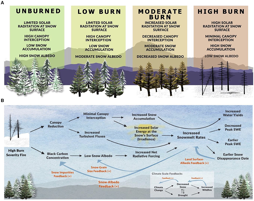
Frontiers Wildfire impacts on western United States snowpacks

Left) X-ray image of a line pair rule taken using an un-collimated

Hans ANDERSSON, Principal Research Engineer

The outline of bump bond process steps. (1) deposition of field metal

Materials, Free Full-Text

Development of an Indium bump bond process for silicon pixel detectors at PSI - ScienceDirect

solder bump flip chip bonding for pixel detector hybridization

Process development for the hybrid additive manufacturing of metallic structures on polymer substrates - ScienceDirect

The outline of bump bond process steps. (1) deposition of field metal

PDF) GaAs array fabrication
AFM Exclusive
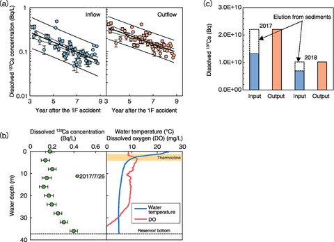
1-14 Remobilization of Radiocesium from Sediments


:fill(ffffff)/http%3A%2F%2Fstatic.theiconic.com.au%2Fp%2Fbonds-6616-368799-1.jpg)