A review on numerical approach of reflow soldering process for copper pillar technology

The Analysis for Bump Resistance Improvement by Optimizing the Sputter Condition

Figure 6 from Under Bump Metallurgy (UBM)-a technology review for flip chip packaging

61387 PDFs Review articles in SOLDERING

UBM (under bump metallurgy) structure
Pb-Free Solders for Flip-Chip Interconnections

PDF) Under bump metallurgy (UBM) - A technology review for flip chip packaging

Intermetallic compounds in 3D integrated circuits technology: a

UBM (under bump metallurgy) structure

The surface characteristics of under bump metallurgy (UBM) in electroless nickel immersion gold (ENIG) deposition - ScienceDirect

Effects of Under Bump Metallurgy (UBM) Materials on the Corrosion of Electroless Nickel Films

The surface characteristics of under bump metallurgy (UBM) in electroless nickel immersion gold (ENIG) deposition - ScienceDirect

Bumps Vs. Hybrid Bonding For Advanced Packaging
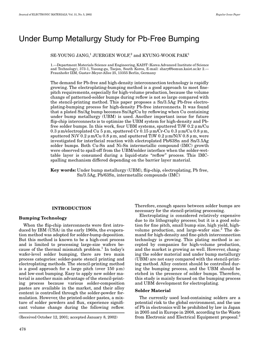
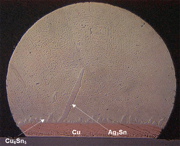
PDF) Under bump metallurgy study for Pb-free bumping
Artificial intelligence deep learning for 3D IC reliability prediction