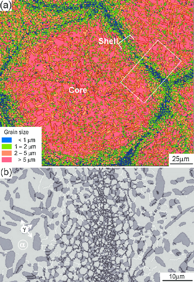
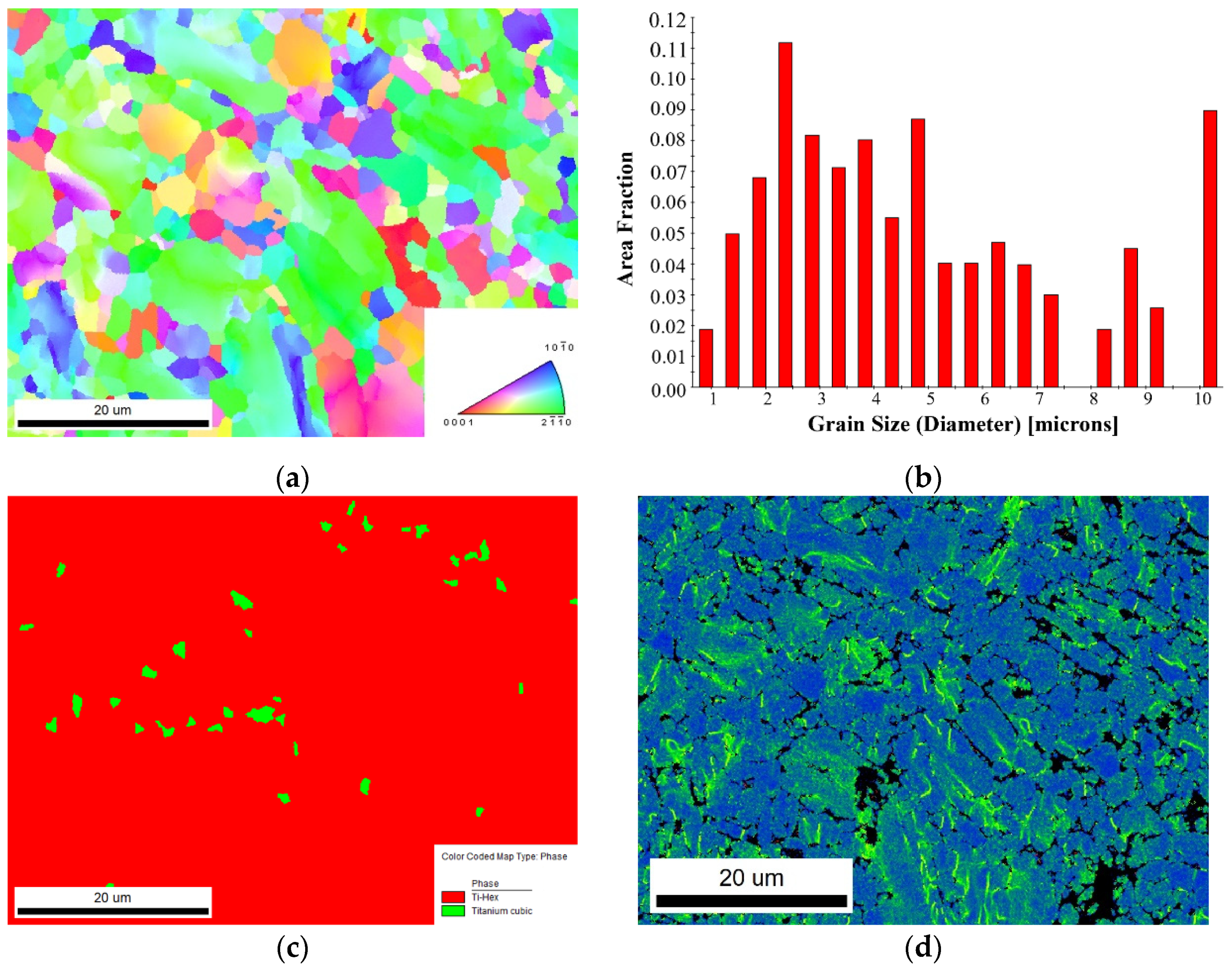
A grain size map (a) and a phase map (b), which is combined with
$ 7.99
4.5(387)In stock
Customer Journey Maps: How to Create Really Good Ones [Examples + Template]
Crystallographic Orientation Analysis of Nanocrystalline Tungsten Thin Film Using TEM Precession Electron Diffraction and SEM Transmission Kikuchi Diffraction, Microscopy and Microanalysis
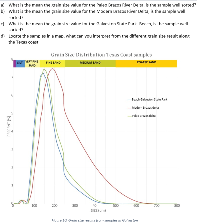
Solved a) What is the mean the grain size value for the
Electron backscatter diffraction - Wikipedia
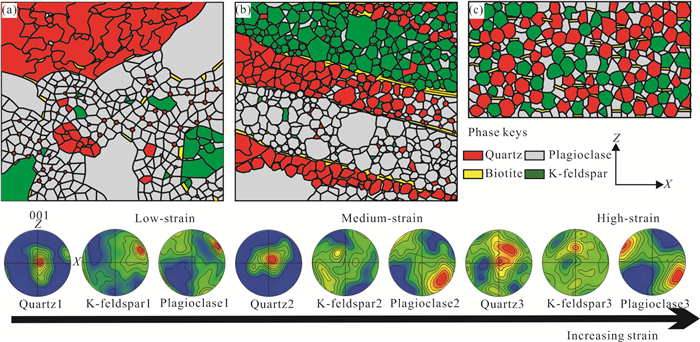
Strain Localized Deformation Variation of a Small-Scale Ductile Shear Zone
Multiscale architectured materials with composition and grain size gradients manufactured using high-pressure torsion
A grain size map (a) and a phase map (b), which is combined with the
e The phase map (a, b), grain map (c, d) and boundary map (e, f) of the
Micromachines, Free Full-Text
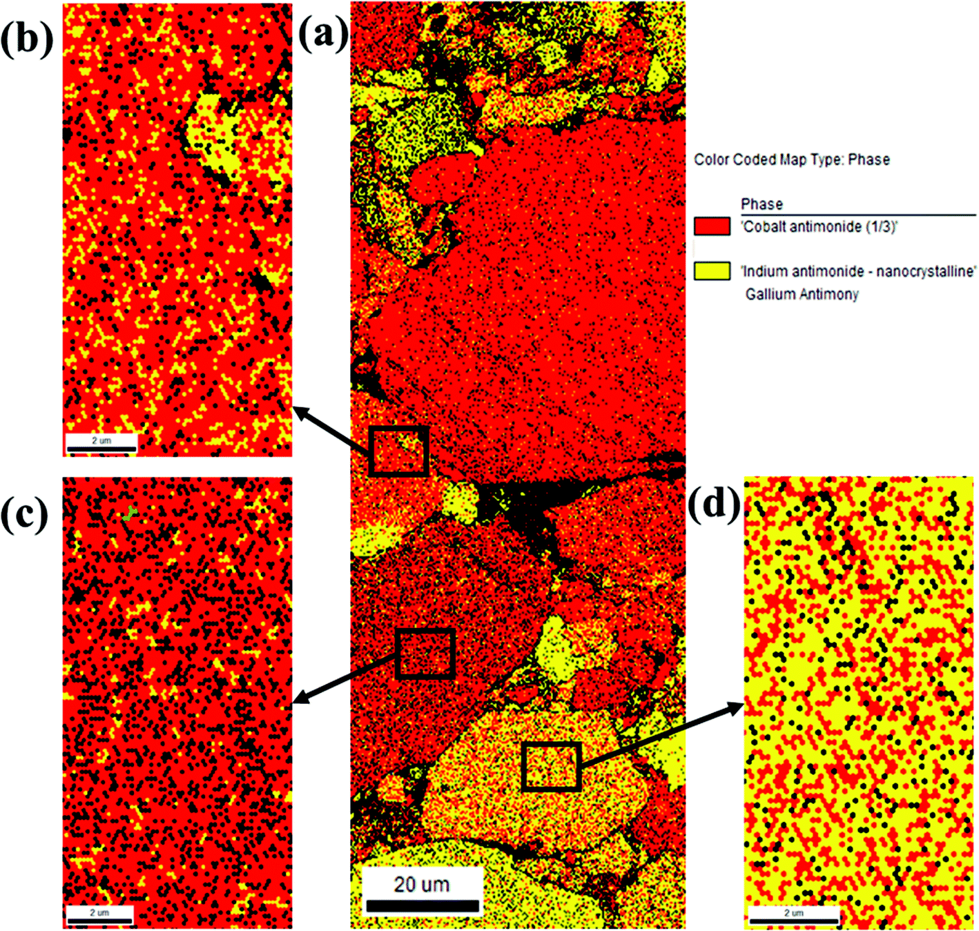
Preferential phonon scattering and low energy carrier filtering by interfaces of in situ formed InSb nanoprecipitates and GaSb nanoinclusions for enha - Dalton Transactions (RSC Publishing) DOI:10.1039/D0DT03429K
PDF) Harmonic Structure Design of a SUS329J1 Two Phase Stainless Steel and Its Mechanical Properties
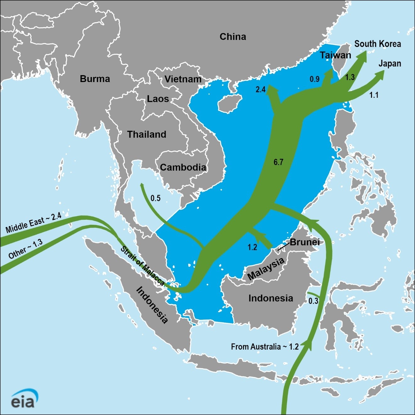
International - U.S. Energy Information Administration (EIA)